
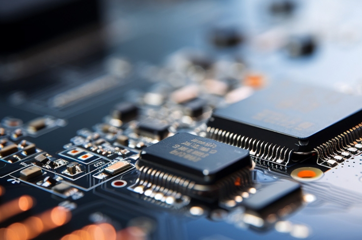
In today’s era of rapid technological development, the semiconductor industry has become the focus of global attention. In this industry, CNC machining technology plays a vital role, providing precise and efficient production tools and components for semiconductor manufacturing. CNC machining is a technology that uses computer-controlled mechanical tools for precise cutting and forming. In the semiconductor industry, this technology is mainly used to produce molds and dies for silicon wafers, which is the cornerstone of semiconductor production. The quality of silicon wafers directly affects the performance and output of chips, so the precision of molds is extremely high, which is exactly the strength of CNC machining.
In addition, CNC machining is also used to manufacture various key components on semiconductor production lines, such as spindles, precision platforms, etc. These components must be able to withstand extreme production environments, including temperature changes, chemical corrosion, and continuous high-speed operation. CNC machining, with its excellent manufacturing accuracy and repeatability, ensures that these components can meet strict industrial standards.
Content:
1. What are the CNC Machining Methods Commonly Used in the Semiconductor Sector?
2.What Are the Common Applications of CNC Machining in the Semiconductor Industry?
3.What are Key Challenges in CNC Machining for the Semiconductor Industry?
4.Future Trends in CNC Machining for Semiconductor Applications
Part One: What are the CNC Machining Methods Commonly Used in the Semiconductor Sector?
In the semiconductor field, the application of CNC machining methods is crucial to improving production efficiency and ensuring part accuracy and quality. The following are several CNC machining methods commonly used in this field:
1. Precision milling
High-precision control: Precision milling uses high-speed precision tools to perform fine processing under CNC control to achieve high-precision processing of silicon wafers and other semiconductor materials.
Complex shape processing: This method is suitable for parts that need to be processed with complex shapes and fine features, such as semiconductor molds and chip heat sinks.
2. Micromachining
Micro-size: Micromachining focuses on processing needs of extremely small sizes, such as drilling of tiny apertures and milling of tiny structures, which is essential for semiconductor packaging and micro-sensor manufacturing.
High-precision positioning: Through precisely controlled machine tool movement, micromachining can achieve high-precision positioning and processing, meeting the semiconductor industry’s stringent requirements for precision.
3. Electrochemical machining
Material removal: Electrochemical machining is a non-contact machining method that removes material through electrochemical reaction. It is suitable for materials with higher hardness, such as tungsten and steel.
Surface quality: This method can provide good surface quality and stress-free processing, which is advantageous for some special material processing in the semiconductor industry
4. Laser cutting
High-energy laser beam: Laser cutting uses a high-energy laser beam to cut materials, which is suitable for fast cutting of thin silicon wafers and semiconductor materials.
Fine cutting: Laser cutting can achieve very fine and precise cutting, which is particularly important for the manufacture and segmentation of semiconductor chips.
5. Ultrasonic machining
Hard material machining: Ultrasonic machining uses high-frequency vibrating tools to process hard materials such as ceramics and silicon, and is suitable for micro-pore and micro-structure manufacturing in the semiconductor industry.
No heat-affected zone: This machining method produces almost no heat-affected zone, which is very important for temperature-sensitive semiconductor materials
6. Precision Grinding
Ultra-high precision surface: Precision grinding is used to produce parts with ultra-high precision surfaces, such as semiconductor molds and wafers, ensuring the quality of the product.
Material integrity maintenance: The grinding process can maintain the integrity of the material, avoiding micro cracks and damage, which is crucial to ensuring the reliability of semiconductor products.
7. High-speed cutting
High-efficiency production: High-speed cutting improves the production efficiency of parts in the semiconductor industry by using high-speed rotating tools to perform fast cutting under CNC control.
Reduced thermal deformation: High-speed cutting reduces thermal deformation caused by slow cutting speed and ensures the processing accuracy of parts.
8. Composite machining
Multi-process integration: Composite machining integrates multiple machining technologies into one CNC machine, such as milling and turning, to improve machining efficiency and accuracy.
One-stop solution: This approach provides a one-stop machining solution for the semiconductor industry, reducing the number of transfers of parts between different machine tools, reducing errors and costs.
9. Mechanical etching
Precision material removal: Mechanical etching removes materials by physical means and is suitable for the manufacture of precision patterns and structures in the semiconductor industry.
No chemical waste: Compared with chemical etching, mechanical etching does not produce harmful chemical waste and is an environmentally friendly processing method
10. Ion beam machining
Micro-nano processing: Ion beam machining is capable of material removal at the micro-nano level, which is of great significance for the miniaturization and precision manufacturing of semiconductor devices.
Precise control: This method allows precise control of machining depth and position, and is suitable for high-precision applications in the semiconductor industry.
The application of these CNC machining methods in the semiconductor industry not only improves production efficiency and product quality, but also promotes the continuous innovation and development of semiconductor technology. With the continuous advancement of technology, CNC machining will continue to play a key role in the semiconductor field.
Part Two: What Are the Common Applications of CNC Machining in the Semiconductor Industry?
In the semiconductor industry, the application of CNC machining technology is extensive and critical. The following are the main application areas:
1. Silicon wafer manufacturing
The molds and blades used to produce silicon wafers can be manufactured by precision milling and grinding using CNC machines. These tools require extremely precise dimensions and smooth surfaces to ensure the quality of the wafers.
2. Semiconductor equipment parts
CNC machining is used to manufacture and maintain precision parts in semiconductor production equipment, such as vacuum chambers, electrodes, and brackets. These parts must have high precision and high reliability to ensure a smooth production process.
3. Packaging and testing equipment
During the packaging and testing stage of semiconductors, CNC machining is used to manufacture molds and frames for chip packaging, as well as precise fixtures and probe cards required in the testing process.
4. Thermal Management System
CNC machining is also used to manufacture thermal management system components in semiconductor manufacturing, such as heat sinks and cooling channels. These components are critical to keeping the temperature of the equipment stable.
5. Precision mechanical parts
Parts such as precision robotic arms and positioning systems in semiconductor manufacturing require CNC processing to ensure their precise movement and positioning.。
6. Optical component manufacturing
In the semiconductor lithography process, CNC machining is used to manufacture optical components such as lenses and mirrors, which are critical to controlling light beams and image quality.。
7. Circuit Board Production
CNC machining also plays a role in the production of circuit boards (PCBs), used to make holes in the boards and cut the shapes of the boards.
8. Research and Development
In the field of semiconductor research and development, CNC machining is used to manufacture prototypes and experimental equipment to help scientists and engineers test and verify new semiconductor designs.
Part Three: What are Key Challenges in CNC Machining for the Semiconductor Industry?
Key challenges facing CNC machining in the semiconductor industry include:
Requirements for precision
The semiconductor industry has extremely strict requirements for precision. Any tiny error may lead to degradation of product performance. CNC machining must achieve sub-micron accuracy to ensure the performance of parts and components.
High material hardness
The materials used in many semiconductor applications are extremely hard, such as silicon and ceramics, which places higher demands on CNC machine tools and cutting tools, requiring the use of high-performance cutting tools and processing methods with low wear.
Complex Geometries
Parts in semiconductor devices often have complex geometries, which requires CNC programming and machining technology to be able to handle complex designs and high-precision manufacturing requirements.
Temperature Control
During the machining process, temperature control is critical because high temperatures may affect the microstructure and precision of the material. CNC machining must be able to be performed under temperature control conditions.
Cleanliness requirements
Semiconductor manufacturing has extremely high requirements for environmental cleanliness to prevent dust and contaminants from damaging the product. The CNC processing area must maintain extremely high cleanliness standards.
Cost pressure
As market competition intensifies, cost control has become a major challenge for CNC machining in the semiconductor industry. Manufacturers need to constantly look for more cost-effective production methods while ensuring quality and precision.
Rapid technological change The semiconductor industry is undergoing rapid technological changes, and CNC processing technology and equipment must be constantly upgraded to adapt to new manufacturing needs and materials.
Talent shortage
There is a relative shortage of professional and technical personnel with advanced CNC operation skills and programming knowledge, which poses a challenge to improving CNC processing efficiency and quality.
Part Four: Future Trends in CNC Machining for Semiconductor Applications:
With the continuous advancement of technology and changes in market demand, the future trends of CNC machining in semiconductor applications may include the following aspects
Intelligence and Automation
CNC machining will further enhance its intelligence and automation level, and through the integration of machine learning and artificial intelligence algorithms, it will achieve automatic programming, real-time monitoring and fault prediction, and improve production efficiency and safety.
Precision micro-nano processing
With the advancement of miniaturization and nanotechnology, future CNC processing technology will be able to achieve higher-precision micro-nano processing to meet the semiconductor industry’s needs for tiny size and high precision.
Application of high-performance materials
New high-performance materials, such as silicon carbide and gallium nitride, will be increasingly used in semiconductor manufacturing. CNC machining technology needs to adapt to the processing requirements of these new materials to achieve efficient and precise manufacturing.
Advanced Cooling Technology
To improve machining accuracy and extend tool life, future CNC machining may adopt advanced cooling technologies such as cryogenic cooling and minimum quantity lubrication (MQL) technology.
Multifunctional integration
Future CNC machine tools may be multifunctional integrated equipment, which can complete the entire process from rough machining to finishing on a single platform, improving flexibility and production efficiency.
Combination of additive and subtractive manufacturing
Hybrid processing technology that combines additive manufacturing (such as 3D printing) and subtractive manufacturing will become a trend, providing new solutions for the manufacturing of complex parts in the semiconductor industry.
Cross-industry collaboration
CNC machining will work more closely with other disciplines such as mechanical engineering, materials science, and electronic engineering to promote the innovative development of semiconductor technology and manufacturing processes.
In short, future CNC machining will be more efficient, precise, and environmentally friendly, providing strong technical support for the development of the semiconductor industry
Post time: Jul-24-2024